
Certain current flows in forward bias mode. The electrons must be pushed by a voltage with enough force to cross the p-n junction and this push is the source of the diode forward voltage or forward bias voltage drop.

Forward Bias Characteristics Of Diode For Laboratory Id 21770694948
Motor Control Electronics Part A

1
However the voltage present across a diode during reverse biasing does not produce any significant flow of current.

Forward bias diode. In forward bias signal diode acts as closed switch and thus short circuited for driving current solely in one direction from the positive terminal to the negative terminal. Forward Bias vs. The biasing of a diode depends upon the direction of.
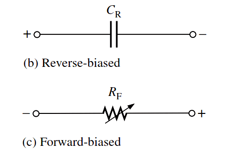
If the voltage moves in the opposite direction we call that orientation a reverse bias In reverse bias current flow is nominally blocked as a sort of electronic check valve. Charge storage effects are modeled by a transit time TT and a nonlinear depletion layer capacitance which is determined by the parameters CJO VJ and M. There is a definite forward voltage at which the diode starts to conduct significantly.
In the reverse bias condition the Zener diode is an open circuit and only a small leakage current is flowing as shown on the exaggerated plot. This is the off mode of the diode where. If this external voltage becomes greater than the value of the potential barrier approx.
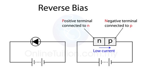
Reverse-bias is when the anode is negative and the cathode is positive. 07 volts for silicon and 03 volts for germanium the potential barriers opposition will be overcome and current will start to flow. The forward resistance is classified as Static Forward Resistance and Dynamic Forward Resistance.
A very small amount of current flows if a diode is reverse-biased. Forward Bias Diode Configuration. Note The current in the diode when flow in the forward direction is called forward current.
If the polarity of the circuit is reversed and the attempt is made to inject electrons into the p-zone while they are removed from the n-zone the diode is said to be reverse biased and no current will flow. The DC characteristics of the diode are determined by the parameters IS N and the ohmic resistance RS. The typical forward voltage at room temperature with a current of around 1 mA is around 06 volts.
With a small forward bias where only a small forward current is conducted the current-voltage curve is exponential in accordance with the ideal diode equation. If the batterys polarity is reversed the diode becomes reverse-biased and drops all of the batterys voltage leaving none for the lamp. To produce diode clipping circuits for voltage waveforms at different levels a bias voltage V BIAS is added in series with the diode to produce a combination clipper as shown.
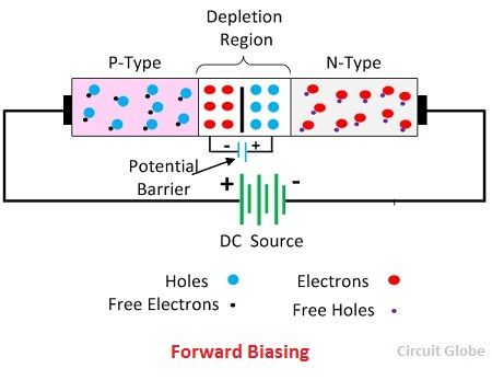
In a forward bias setup the P-side of the diode is attached to the positive terminal and N-side is fixed to the negative side of the battery. When the voltage across the diode is positive the diode is on and current can run through. The depletion layer of the diode is very thin in forward biasing and thick in reverse bias.
Reverse bias and little or no concern for carrier lifetime Stored ChargeWhen the forward bias control current of the PIN diode is varied continuously it can be used for attenuating leveling and amplitude modulating an RF signal. The name tunnel diode is due to the quantum mechanical tunneling is responsible for the phenomenon that occurs within the diode. A lot of current flows when the diode is forward-biased provided that the voltage is higher than 06V or so for a silicon diode or 03V or so for a germanium device.
In the current voltage characteristics of tunnel diode we can find a negative slope region when a forward bias is applied. When a forward bias is applied to the diode then it causes a low impedance path and permits to conduct a large amount of current which is known as infinite current. When the diode is in reverse bias and it is unable to conduct current the output of the circuit is nearly zero volts.
In a standard diode forward biasing occurs when the voltage across a diode permits the natural flow of current whereas reverse biasing denotes a voltage across the diode in the opposite direction. Maximum average forward current IFAV the maximum average amount of current the diode is able to conduct in forward bias mode. The pn junction is also abrupt.
Negligible current flows in reverse bias mode until zener or avalanche breakdown happens. We will connect the diode in forward bias so that the forward current and the forward voltages will flow through the series circuit. If the diode in a series clipper circuit is in forward bias condition then the output waveform at the load follows the input waveform.
The voltage across the series combination must be greater than V BIAS 07V before the diode becomes sufficiently forward biased to. This current starts to flow above the knee point with a small amount of external potential. Forward bias or biasing is where the external voltage is delivered across the P-N junction diode.
Forward Voltage and Breakdown Voltage. Diodes nominally conduct electricity in one direction and the voltage they apply follows a so-called forward bias orientation. In reverse bias silicon diode acts as open switch and thus open circuited for blocking the current flowing in the diode.
This is fundamentally a thermal limitation. When a diode is connected in a Forward Bias condition a negative voltage is applied to the N-type material and a positive voltage is applied to the P-type material. The forward bias has large forward current while the reverse bias has very small forward current.
The forward bias region of a Zener diode is identical to that of a regular diode. Furthermore reverse-bias voltage does induce a small amount of current through the diode called leakage current that is essentially negligible for most purposes. Static or DC Forward Resistance.
Understanding the Q point of a diode enables better circuit current functionality. The forward-bias and the reverse-bias properties of the pn junction imply that it can be used as a diode. A forward-biased diode conducts current and drops a small voltage across it leaving most of the battery voltage dropped across the lamp.
For this reasons the depletion layer width is very small. Negative charges electrons can easily flow through the junction from n to p but not from p to n and the reverse is true for holes. The opposition offered by a diode to the direct current flowing forward bias condition is known as its DC forward resistance or Static Resistance.
The voltage should be greater than the forward voltage V F in order for the current to be anything significant. How much heat can the PN junction handle given that dissipation power is equal to current I multiplied by voltage V or E and forward voltage is dependent upon both current and junction temperature. As per the Kirchhoffs current law the current flowing through the diode ID and the resistor IR are equal ID IR.
Forward Bias Zener or Voltage Avalanche Breakdown PN junction diode acts as a rectifier as seen in the IV characteristic. The half wave rectifier circuit is similar to a series clipper circuit. A pn junction diode allows electric charges to flow in one direction but not in the opposite direction.
The forward bias diode works like a closed switch and allows the current through itselfIn contrast to the forward bias the reverse bias diode blocks the current passage and works as an open switch. A diode is two terminal electronics components which can be connected to the source in two different ways. When the control current is switched on and off or in discrete steps the device.
There is a minimum threshold voltage required to overcome the depletion region which for most silicon diodes is a significant 07 volts. Forward Bias and Reverse Bias.
Difference Between Forward Reverse Biasing With Comparison Chart Circuit Globe
Reverse Bias Working Principle Of Junction Diode Qs Study
Voltage Drop Diode Reverse Biased Electrical Engineering Stack Exchange
Pin Diode Working Principle Inst Tools

What Is Forward Bias And Reverse Bias Example Applications Etechnog
Zener
What Are Forward Biased And Reverse Biased Diodes Quora
Pn Junction Diode And Diode Characteristics


